What are the design criteria for chip applications
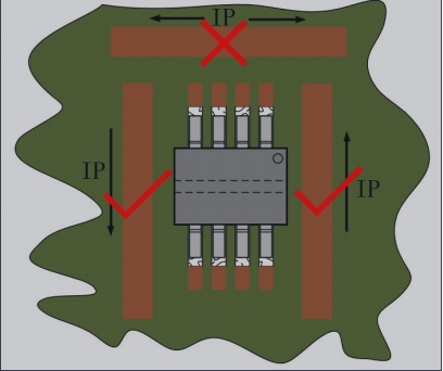
Attention should be paid to minimize the inductance of the measured current path. In addition, contact / connection resistance in this path should be minimized. In PCB design, the measured current path should be perpendicular to the chip as far as possible to reduce the stray magnetic field interference generated by the current line, as shown in the figure below.


 联系电话
联系电话